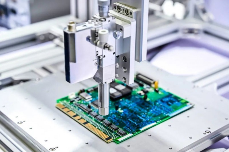
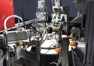
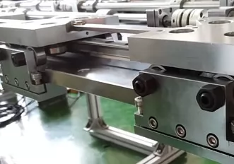
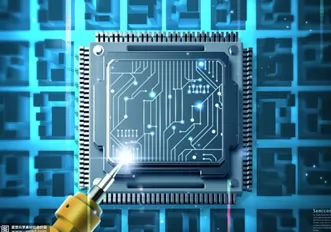
In wafer handling equipment, linear guides are used to precisely position and transfer semiconductor wafers through various stages of the manufacturing process. The precision required in this equipment is high, with tolerances often being in the sub-micron range.
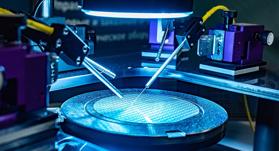
Wafer inspection systems also use linear guides to provide precise and smooth movement of inspection tools, enabling high-precision measurements and detection of defects in the wafer surface.
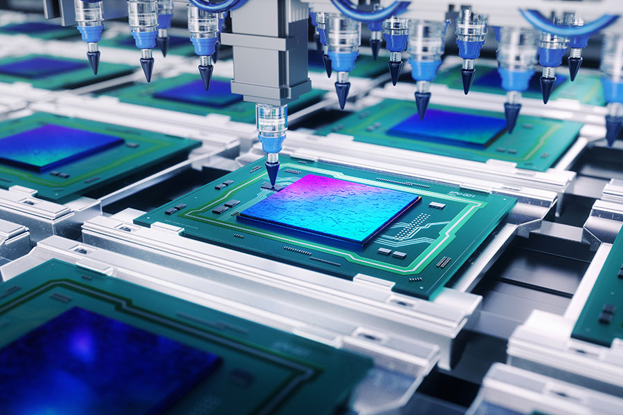
Photolithography equipment, which is used in the semiconductor manufacturing process to pattern the surface of wafers, also requires high precision linear guides to ensure accurate positioning of the wafer and exposure of the pattern.
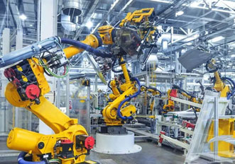
In the semiconductor industry, linear guides are used for their excellent accuracy, high stiffness, and low friction. These properties enable the equipment to operate with high precision and repeatability, leading to high-quality manufacturing results. With the increasing demand for miniaturization and high performance of electronic devices, the need for linear guides in the semiconductor industry is expected to continue to grow.
 +8615622924499
 +8615622924499

